|
China Laptop Charger Online Market Group
|
Gold Index: 7547


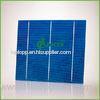
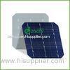
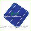
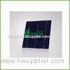
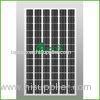
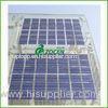
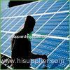
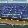
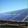
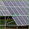
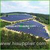
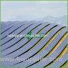
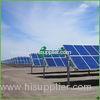
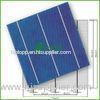
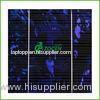
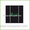
P Type Monocrystalline Solar Cells
| Place of Origin: | Zhejiang, China (Mainland) |
|
|
|
| Add to My Favorites | |
| HiSupplier Escrow |
Product Detail
<table align="left" border="1" cellpadding="2" cellspacing="0" style="background-color:rgb(230, 230, 250); border-style:hidden; whi
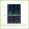
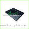
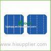
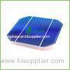
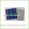
| Materials | Monocrystalline Silicon | Size | 125*125mm |
| Max.power | 2.86W | Type | N type |
| Grade | A Grade | Warranty | 25 years |
| Efficiency | 18.4%-17.0% | Busbar | 2 bus bar |
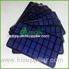
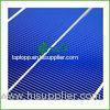
| Producion Capacity | 150MW / year | Color | Deep blue |
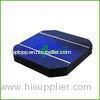
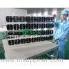
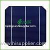
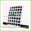
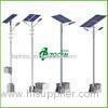
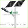
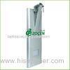
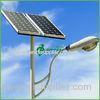
Monocrystalline Solar Cells, Size Of 125*125mm 2BB, High Efficiency
1> Quick Detail:
- Place of Origin: China
- Brand Name: ZOCEN
- Model: ZC TDB-125*125
- Certificate: CE,CQC, IEC, TUV, CEC, MCS, CHUBB, ISO9001
2> Description:
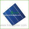
- Mono-crystalline Silicon
A single-crystal silicon - often made using the Czochralski process - mono-crystalline wafer cells are generally expensive.
The expense arises as mono-crystalline wafers are cut from cylindrical ingots.
As a result, the silicon wafers do not entirely cover the surface of a square solar cell module without a substantial waste of refined silicon. Hence most mono-crystalline panels have uncovered gaps at the four corners of the cells.
-
Fabrication
Once the solar cell is fabricated, that is, once it has been either grown or the layers of the solar cell have been deposited onto each other, and you’re looking at a wafer, the front and back contacts need to be added to give the electron-hole pairs a place to go and complete the photoelectric effect… That is, wires need to be added to allow current to flow!
This is a place where things get tricky and lots of research is being done, because when the deposition of a metal layer onto a crystal is done, at the boundaries between the two materials a resistance exists that is generally larger than the resistance inside the homogeneous material itself. The research is to reduce this resistance with various theories and tricks.
-
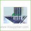
Application
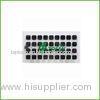
Each solar cell wafer is generally combined into one big solar panel, which is most likely what you buy in the stores. These are usually all wired up, and ready for you to plug into a battery!
- Materials: Mono silicon
- Format Dimension: 125 x 125mm (±0.5mm)
- Diagonal: R165mm
- Thickness wafer (Si): 190±20μm
- Thickness cell: 200±40μm
- Weight: 12g
- High efficiency: 18.4%-17.0%, stable performance conversion
- Front(-): Blue silicon nitride anti-reflection coating 1.8mm silver busbars
- Back(+): Full-surface aluminum back-surface field 2.5mm(silver/ aluminum) continuous soldering pads Efficiency range: 17.0-18.4%
- Maximum power range: 2.86 to 2.69W
- Grade type: A
- Typical temperature coefficients: Voltage: -0.038%/K; Current: +0.031%/K; Power: -0.46%/K
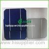
3> Zocen 5" Monocrystalline Solar Cell
- Product details
- Materials: Mono silicon
- Format Dimension: 125 x 125mm (±0.5mm)
- Diagonal: R165mm
- Thickness wafer (Si): 190±20μm
- Thickness cell: 200±40μm
- Weight: 12g
- High efficiency: 18.4%-17.0%, stable performance conversion
- Front(-): Blue silicon nitride anti-reflection coating 1.8mm silver busbars
- Back(+): Full-surface aluminum back-surface field 2.5mm(silver/ aluminum) continuous soldering pads Efficiency range: 17.0-18.4%
- Maximum power range: 2.86 to 2.69W
- Grade type: A
- Typical temperature coefficients: Voltage: -0.038%/K; Current: +0.031%/K; Power: -0.46%/K
- Features:
- High conversion efficiencies resulting in superior power output performance.
- Suitable for keeping appearance of solar cell tidy and clean.
- Advanced diffusion technology adapted to ensure conversion efficiency uniformity throughout cell.
- Advanced PECVD film forming technology used to coat cells with dark blue silicon nitride anti-reflection coatings.
- Uniform color appearance.
- Advanced soft line and high precision silkscreen printing equipment to achieve high smoothness, make automatic welding and laser cutting easier.
- Metal paste applied to making back surface field and electrode to ensure top conductivity, nice adhesion, superior weld-ability, nice appearance and reliable performance.
- Efficiency, stability and durability of crystal silicon.
- Low breakage rate.
- Environmental protection.
- OEM orders are welcome
4> Specifications:
-
Mechanical dimensions

- Electrical Parameters of products
|
Product name |
Efficiency(%) |
Pmpp(W) |
Vmpp(V) |
Impp(A) |
Voc(V) |
Isc(A) |
| 125*125mm(5") Mono-Crystalline Silicone Solar Cell | 18.4 | 2.86 | 0.532 | 5.372 | 0.630 | 5.721 |
Related Search
Monocrystalline Silicon Solar Cells
Solar Cells
Monocrystalline Solar
Polycrystalline Solar Cells
Solar Power Cells
Solar Panel Cells
More>>
Find more related products in following catalogs on Hisupplier.com
Company InfoChina Laptop Charger Online Market Group [China (Mainland)]
Business Type:Manufacturer You May Like:
Printable Page
Bookmark this page
Sitemap XML About HiSupplier Help Center Customer Service Friend Links Site Map Archives Browse by: China Suppliers - Hot Products - Products Directory - Offers Directory - Suppliers Directory - Buyers Directory Language Option: العربية - Nederlands- Français- Deutsch- Italiano- 日本語- 한국의- Português- Pусский- Español Copyright © HiSupplier.com Online Inc. All Rights Reserved.

|